Have you ever spent hours perfecting a PCB layout in Proteus only to end up with a blurry, misaligned print that ruins your copper board? You're not alone — and this guide gives you the exact fix. Learning how to print PCB layout Proteus the right way separates makers who waste boards from those who nail clean, precise transfers every single time. Whether you're etching your first board or streamlining a production workflow, the print settings inside Proteus matter more than most tutorials admit. Our team at ShopChrisAndMary covers everything from art and craft printing to professional electronics workflows — so you're in the right place to get this right.
Proteus is one of the most widely used PCB design and simulation platforms in electronics education and professional labs. Its print output options are far more powerful than most users realize. The problem is that default settings almost never match what your printer, your paper, or your toner transfer process actually needs. You need to know exactly which layers to export, whether to mirror your artwork, what scale to lock in, and what media to load — each of those decisions directly affects your final board.
This guide covers all of it: the Proteus print dialog, the best paper and printer choices, the mistakes that ruin boards, and the myths that trip up even experienced designers. By the end, you'll have a clear, repeatable process you can trust every time you sit down to etch.
Contents
Why Proteus Is the Standard Tool for PCB Design and Printing
What Sets Proteus Apart
Proteus, developed by Labcenter Electronics, is a combined schematic capture, PCB layout, and circuit simulation tool. It's a staple in universities and maker labs because you get a complete design-to-print pipeline inside a single application — no need to export to a third-party layout tool just to generate printable artwork. Proteus ARES handles multi-layer PCB design with fine-grained control over which layers appear in your print output.
- Supports single-sided, double-sided, and multi-layer boards
- Exports individual copper layers, silkscreen, and drill guides separately
- Integrates circuit simulation so you validate before you fabricate
- Widely used across hobby, educational, and professional electronics contexts
- Exports industry-standard Gerber files for professional PCB fabrication
The key advantage over simpler CAD tools is that Proteus gives you explicit layer control at print time. You choose exactly what goes on paper — and that precision is what makes clean DIY etching possible.
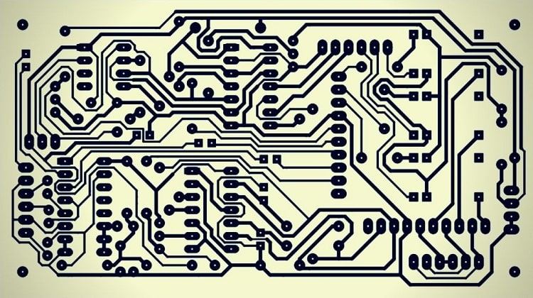
Understanding PCB Layers Before You Print
Before you open the print dialog, you need a clear picture of which layers matter for your specific output. Print the wrong combination and you'll produce unusable artwork, no matter how clean your design is.
| Layer Name | Purpose | Print for DIY Etching? | Mirror Required? |
|---|---|---|---|
| Bottom Copper (B.Cu) | Main conductive trace layer for single-sided boards | Yes — primary artwork | Yes |
| Top Copper (F.Cu) | Top-side traces for double-sided boards | Yes — secondary artwork | No |
| Board Edge | PCB outline and boundary | Yes — helps with cutting | Same as copper layer |
| Silkscreen | Component labels and reference designators | Optional (reference only) | No |
| Drill Guide | Marks drilling positions for through-hole components | Yes — separate print | No |
For a standard single-sided DIY board, you only need the bottom copper layer — mirrored — plus the board edge. Print anything else on the same page and you'll create visual confusion during transfer or etching. Keep it simple. One layer at a time.
How to Print PCB Layout from Proteus: Step-by-Step
Setting Up the Print Dialog
Getting the print dialog right is where most beginners fail. Follow these steps exactly and you'll sidestep the most common failure points when you need to print PCB layout from Proteus:
- Open your completed PCB layout in Proteus ARES.
- Go to Output → Print Layout (keyboard shortcut: Ctrl+P in ARES).
- In the Print dialog, locate the Layers panel on the left side.
- Deselect all layers first — then check only Bottom Copper and Board Edge for a single-sided board.
- Enable the Mirror checkbox. This is non-negotiable for toner transfer — skip it and your traces reverse on the board.
- Set Scale to 1:1 (100%). Never allow the printer to auto-scale your artwork.
- Set the color mode to Black and White — color output is useless for etching.
- Click Preview before committing. Confirm you see only one copper layer with solid filled pads.
- Send to printer — or export to PDF for an extra verification step.
Scale, Mirror, and Fit-to-Page Settings
Scale is the single most critical variable in the entire process. A print at anything other than 1:1 produces a board that doesn't match your component footprints. Verify scale in the preview window by checking a known dimension — the pad pitch of a standard DIP IC is exactly 2.54mm. Measure it on paper after printing.
- Disable "Fit to Page" — this silently scales your layout to fill the paper and is on by default in many printer drivers.
- Use A4 or US Letter depending on your board size and regional paper standards.
- For large boards that exceed a single sheet, our guide on printing across multiple pieces of paper shows you how to tile your layout accurately across sheets.
- Always run a test print on plain copy paper before using expensive transfer media — confirm dimensions first.
Export to PDF vs. Direct Print
You have two output paths in Proteus: print directly to your connected printer, or export to PDF and print from a viewer. PDF export is the better option for most users. Here's why:
- PDF preserves exact scale — no surprises from printer driver rescaling.
- You can inspect the artwork on screen before any paper is used.
- Files are easy to archive and reprint without reopening Proteus.
- Adobe Reader and most PDF viewers have an "Actual Size" (100%) print option that guarantees accurate output.
If you print directly, open your printer's Properties dialog and disable every "Scale to Fit," "Shrink Oversized," or "Fit to Printable Area" option you find. Those settings exist for documents, not precision artwork.
Laser vs. Inkjet: Which Printer Works Best for PCB Layouts
Why Laser Printers Dominate for Toner Transfer
The toner transfer method — the most popular DIY PCB etching technique — works only with laser printers. Inkjet ink soaks into paper fibers and smears under the heat needed for transfer. Laser toner is a dry powder that fuses to the paper surface, making it transferable to copper when heat and pressure are applied correctly.
- Use a laser printer with a minimum of 600 DPI for clean fine-pitch traces.
- Set printer darkness or toner density to maximum — thin toner layers don't transfer completely.
- Monochrome laser printers are faster and more consistent than color laser for PCB artwork.
- Check our best duplex laser printer reviews for models that perform reliably on specialty transfer media.
- Avoid off-brand compatible toner cartridges — inconsistent toner density causes trace breaks mid-etch.
For the transfer paper itself, our detailed guide on how to print on iron-on transfer paper walks through paper types, iron temperature, pressure technique, and peeling — all of which directly affect whether your traces land clean on the copper.
When Inkjet Printing Works for PCB Output
Inkjet printers aren't completely off the table. They're useful in specific, limited scenarios:
- Component placement reference overlay: A full-color diagram you keep next to the board while soldering.
- Drill templates: A printed guide for hand-drilling through-hole component positions accurately.
- UV photoresist method: Some photosensitive films accept inkjet-printed transparency film as a mask — though results vary significantly by film sensitivity and brand.
When printing on coated or specialty inkjet media, our guide on how to print on glossy paper covers the media handling and print settings that also apply to inkjet transparency sheets and coated specialty papers.
Pro Tip: Always run your first print on plain copy paper and measure it with calipers before loading glossy transfer paper or film — specialty media is too expensive to waste on an unchecked settings error.
PCB Printing Mistakes That Ruin Boards
Wrong Scale and Mirror Errors
These two mistakes account for the majority of failed DIY boards. Both are avoidable. Both are easy to fix once you know where to look.
- Forgot to mirror: Traces are reversed. Components won't align with pads. You have to reprint and re-etch.
- Scale set to "Fit Page": Your 60mm board printed at 56mm. No component footprint will match.
- Printed wrong layer: Silkscreen instead of copper — you get component outlines with zero trace data underneath.
- Printed both copper layers together: Overlapping top and bottom copper artwork creates an unusable merged image.
- Forgot to deselect ratsnest layer: Extra lines appear across your artwork that aren't real traces.
The fix is consistent: use the Preview button every single time before printing. Confirm only one copper layer is visible and that pads appear as solid, filled shapes — not outlines.
Using the Wrong Paper or Media
Your paper choice directly determines whether toner transfer succeeds. Standard office paper absorbs toner too deeply into its fibers — you'll lose trace detail the moment you apply heat and try to peel.
- Best choice: Glossy photo paper. Toner sits on the surface coating and releases cleanly onto copper under heat and pressure.
- Excellent alternative: Dedicated PCB transfer film, which releases even more cleanly than photo paper and leaves minimal residue.
- Niche option: Some makers use rice paper, which dissolves completely in water after transfer — no scrubbing, no trace damage.
- Avoid: Plain office paper, cardstock, inkjet-coated paper, and any media labeled for inkjet-only use.
For handling similar specialty media in your printer, our guide on printing on clear sticker paper covers the feed settings and tray adjustments that apply to any thin or coated sheet you're running through a laser printer.
Fuser temperature also matters. Set your printer to its highest heat setting. Lower fuser temperatures produce faint toner that ferric chloride eats right through during etching.
Alignment and Registration Issues
Double-sided boards require precise alignment between the top and bottom copper layers. One misregistered sheet means every through-hole via misses its pad on the opposite side.
- Print both layers on the same sheet using a lightbox overlay — print one side, flip the sheet carefully, re-feed it, and print the second side.
- Punch registration holes in all four corners before printing the second side to lock alignment.
- Print a plain-paper overlay of both layers stacked to verify registration before using transfer media.
- For double-sided alignment strategies and media handling on specialty surfaces, our guide on printing on black cardstock covers double-sided feed techniques you can adapt directly to this workflow.
PCB Printing Myths You Need to Stop Believing
Myth: Any Printer Will Do for PCB Toner Transfer
This is the most damaging myth for beginners. Printer type, toner formulation, and fuser temperature all directly affect transfer quality. Some specific misconceptions you'll encounter on forums:
- "My inkjet prints sharper images, so it'll work better." — Wrong. Inkjet ink is water-based and smears under iron heat. Toner is a dry powder that bonds to copper. The output quality of your screen has nothing to do with transfer chemistry.
- "A cheap entry-level laser printer is fine." — Sometimes. Budget models often run at lower fuser temperatures and inconsistent toner density. Test on scrap copper first before committing to a full board run.
- "A color laser printer gives better detail." — No. Color laser printers use a four-pass toner system that can introduce slight misalignment between passes. A monochrome laser is faster, cheaper, and more reliable for single-color PCB artwork.
Myth: Higher DPI Always Means Better PCB Prints
Resolution matters — but it's not the bottleneck you think it is. Above 600 DPI, the gains in trace quality are negligible for most DIY PCB work. What actually determines your output quality:
- Toner density: A 600 DPI print at maximum darkness outperforms a pale 1200 DPI print every time. Thin toner means thin etch resist, which means broken traces.
- Paper quality: The sharpest 2400 DPI print on office paper blurs during transfer. Glossy photo paper at 600 DPI wins by a wide margin.
- Minimum trace width: Standard DIY etching handles traces reliably down to 0.5mm (20 mil). Below that, DPI becomes genuinely relevant — but most hobby projects don't push that far.
Dial in your toner density and paper choice first. Resolution is the last variable to optimize, not the first.
Myth: Proteus Can't Produce Professional-Grade Output
This one stops hobbyists from ever scaling up. Proteus ARES exports fully compliant Gerber and Excellon drill files — the exact format used by every professional PCB fabrication house on the planet. If you're ready to move beyond DIY etching, you don't need to switch tools.
- Use Output → Generate Gerber/Excellon Files in ARES to export a complete fab package.
- The exported files are accepted directly by JLCPCB, PCBWay, OSH Park, and all major manufacturers.
- Your Proteus workflow scales from breadboard prototype to production PCB without changing software.
Frequently Asked Questions
What paper is best for printing a PCB layout from Proteus?
Glossy photo paper is the top choice for the toner transfer method. The toner sits on the glossy surface coating instead of soaking into paper fibers, so it releases cleanly onto the copper board when heat and pressure are applied. Dedicated PCB transfer film works even better but costs more per sheet.
Why does the PCB print from Proteus need to be mirrored?
When you press the printed sheet face-down onto the copper board and apply heat, the image flips. The side that was facing up on paper ends up facing down on the copper. If you don't mirror the artwork in Proteus before printing, your traces and component pads will be reversed on the finished board.
Can I use an inkjet printer to print a PCB layout from Proteus?
Not for the toner transfer method. Inkjet ink is water-based and won't transfer to copper under heat — it just smears. You can use an inkjet to print a component placement reference or a drill guide on plain paper, but the etch-resist artwork itself requires a laser printer.
How do I lock the scale to 1:1 in Proteus ARES?
In the ARES print dialog, set the Scale field to 100% or 1:1, and uncheck any "Fit to Page" or "Scale to Paper" option. After printing on plain paper, verify scale by measuring the pad pitch of a DIP component footprint — it should be exactly 2.54mm (0.1 inch) between pad centers.
Which layers should I select when printing a single-sided PCB from Proteus?
For a single-sided board, select only the Bottom Copper layer with the Mirror checkbox enabled, plus the Board Edge layer so you know where to cut. Deselect all other layers. Silkscreen and drill guides should be printed as separate runs when needed.
Can Proteus export Gerber files for professional PCB fabrication?
Yes. Proteus ARES supports full Gerber and Excellon drill file export via Output → Generate Gerber/Excellon Files. These files meet industry standards and are accepted by all major PCB manufacturers including JLCPCB, PCBWay, and OSH Park. You don't need to switch to a different tool to go from DIY etching to professional fabrication.
What DPI should I use when printing a PCB layout from Proteus?
600 DPI is sufficient for most hobby PCBs with trace widths of 0.5mm or larger. At that resolution, toner density and paper quality have far more impact on trace quality than resolution does. Only consider 1200 DPI for very fine-pitch traces below 0.3mm — and even then, media quality remains the limiting factor.
Why are my PCB traces breaking after the toner transfer?
Broken traces after transfer usually come from one of three causes: insufficient heat or pressure during the iron-on step, low toner density from the printer (set your printer to its maximum darkness setting), or plain paper that holds toner too tightly to release. Switch to glossy photo paper, increase your iron temperature, and extend your dwell time to 30–60 seconds with firm pressure.
Next Steps
- Open your Proteus ARES layout right now and run through the print dialog checklist from Section 2 — confirm scale is locked at 1:1, the Mirror checkbox is enabled for bottom copper, and "Fit to Page" is disabled.
- Print a test copy on plain paper and measure the DIP pad pitch with a ruler or calipers to verify your scale is exactly 2.54mm before you touch a sheet of transfer media.
- If you're still using an inkjet for PCB artwork, switch to a dedicated monochrome laser printer — our best duplex laser printer guide lists models with reliable fuser temperature for consistent toner transfer results.
- Stock glossy photo paper or dedicated PCB transfer film, and bookmark our guide on iron-on transfer paper printing for the full ironing, peeling, and inspection workflow that follows your Proteus print.
- Once your DIY etching process is dialed in, export Gerber files from Proteus ARES and upload them to a professional fab house — your Proteus workflow scales directly to production without any tool changes.


About Chris & Marry
Chris and Mary are a couple with a shared background in graphic design and print production who have spent years working with printers across creative and professional contexts — from art printing and photo output to label production and professional document work. Their combined experience evaluating printer performance, color accuracy, and paper handling across inkjet and laser platforms gives them a practical, hands-on perspective on what makes a printer worth buying. At ShopChrisAndMary, they cover printer reviews, buying guides, and recommendations for artists, photographers, and professional users.
Time to get FREE Gifts. Or latest Free printers here.
Disable Ad block to reveal all the info. Once done, hit a button below