Over 50 billion printed circuit boards are manufactured globally each year, yet how to make PCB at home remains one of the most underestimated skills in the electronics hobbyist toolkit. With a laser printer, photoresist-coated copper-clad board, and a handful of chemicals available at any hardware store, you can prototype functional single-sided boards in under two hours. The gap between a rough schematic and a working board has never been smaller. If you're already comfortable with craft-oriented making, check out our art & craft printer guides for more hands-on production techniques that overlap with DIY fabrication.
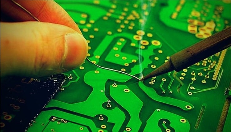
Two proven methods dominate home fabrication: toner transfer and photoresist (UV exposure). Toner transfer is faster and requires less upfront investment. Photoresist produces finer trace resolution — 8 mil and below — which matters the moment you're routing SMD components or dense IC footprints. Both methods share the same core chemistry: protect copper where you want it, dissolve copper where you don't. Understanding that principle makes every troubleshooting step intuitive rather than mysterious.
This guide walks you through the complete workflow — from busting the misconceptions that cause first-timers to fail, to assembling the right toolkit, to executing the toner transfer process step by step. You'll also get a clear framework for deciding when home fabrication is the smart choice and when a PCB service will save you more time than it costs.
Contents
Five PCB Myths Holding Hobbyists Back
Misinformation about home PCB fabrication circulates constantly on forums and outdated tutorials. These myths cause beginners to buy the wrong gear, abandon projects early, or skip home fabrication entirely for boards that would have taken an afternoon to make.
The Inkjet Myth
Inkjet printers cannot perform toner transfer — period. Toner is a dry, heat-fusible polymer powder. Inkjet ink is water-based and does not bond to copper under heat. You need a laser printer or a photocopier for any toner transfer method. An Epson inkjet is useless here, no matter how high the resolution. If you're curious how laser and inkjet technologies differ in practice, our breakdown of Epson solvent printers vs. inkjet printers covers the fundamental output differences in detail.
The Resolution Myth
Many guides claim home fabrication maxes out at 20 mil traces. That's outdated. A modern 600 dpi laser printer running toner transfer on quality glossy paper reliably produces:
- 10–12 mil traces with consistent results
- 8 mil traces with optimized paper and iron pressure
- 6 mil traces using UV photoresist — achievable without professional equipment
The limiting factor is your process discipline, not the technology ceiling.
The Dangerous Chemicals Myth
Ferric chloride is the standard etchant for home PCB work. It stains everything it touches, but it is not acutely hazardous when handled with nitrile gloves and ventilation. Ammonium persulfate is even more benign and easier to dispose of safely. Neither requires a fume hood or a chemistry lab. According to Wikipedia's overview of printed circuit board fabrication, ferric chloride has been the dominant hobbyist etchant for decades precisely because of its accessibility.
Pro tip: Warm your ferric chloride solution to 35–40°C before etching — it cuts etch time from 20+ minutes down to 5–8 minutes and dramatically reduces undercut on fine traces.
Your Complete Home PCB Fabrication Toolkit
You don't need to spend hundreds of dollars. A complete toner transfer setup runs under $50 if you already own a laser printer. Photoresist adds UV exposure equipment but improves yield on complex boards.
Printing Setup
- Laser printer — any monochrome model with adjustable toner density; set to maximum darkness
- Glossy magazine paper or dedicated PCB transfer paper — standard laser paper fails; toner must release cleanly onto copper
- EDA software — KiCad (free), Eagle, or EasyEDA for layout; export as mirrored PDF or Gerber
- Clothes iron or laminator — a laminator provides more consistent pressure than an iron; calibrated heat and pressure is the single biggest variable in transfer quality
Etching Setup
- Copper-clad FR4 board — 1 oz copper weight for most single-sided work
- Ferric chloride or ammonium persulfate — store in a sealed HDPE container
- Plastic etching tank or zip-lock bag — agitation accelerates etching
- Nitrile gloves and safety glasses — non-negotiable
- Acetone — removes toner after etching
- PCB drill bits (0.8 mm, 1.0 mm, 1.2 mm) — carbide bits only; HSS dulls immediately on FR4
Method Comparison
| Factor | Toner Transfer | UV Photoresist |
|---|---|---|
| Minimum trace width | 10–12 mil reliable, 8 mil possible | 6–8 mil reliable, 4 mil possible |
| Setup cost | $15–$40 (consumables only) | $40–$80 (UV box or sunlight) |
| Process time | 45–90 minutes total | 90–150 minutes total |
| Yield on first attempt | 60–70% | 80–90% |
| Best for | Through-hole prototypes, quick iterations | SMD layouts, fine-pitch IC pads |
| Skill ceiling | Moderate — iron/laminator technique matters | Lower — exposure is more consistent |
How to Make PCB at Home: Toner Transfer, Step by Step
This is the core workflow for how to make PCB at home using the toner transfer method. Execute each step precisely — skipping surface prep or rushing the soak is where most failed boards originate.
Design and Print
- Complete your schematic and route traces in KiCad or EasyEDA. Keep trace widths at 12 mil minimum for your first boards.
- Mirror the copper layer before printing — toner side will press directly against copper, so the layout must print as a mirror image.
- Set your laser printer to maximum toner density and disable any toner-saving mode.
- Print onto glossy magazine pages or PCB transfer paper — never standard laser paper.
- Inspect the printout under bright light. Traces must be fully solid black with no gaps or thin spots.
The printing step is analogous to precision craft output — the same way misaligned heat transfer paper ruins a garment, a poor toner print ruins the board. Read up on common mistakes in heat press transfer work for a useful parallel on pressure, temperature, and media compatibility.
Transfer and Etch
- Sand the copper-clad board with 400-grit sandpaper in circular motions until the surface is uniformly matte. Remove all oxidation.
- Clean with acetone on a lint-free cloth. Do not touch the copper surface with bare fingers afterward.
- Place the printout toner-side down onto the copper. Secure edges with small pieces of adhesive tape.
- Apply the iron at 190–200°C (no steam) using firm, even pressure. Work in overlapping strokes for 4–6 minutes.
- Submerge the board in warm water for 3–5 minutes. Gently roll the paper away with your fingertip — do not peel.
- Inspect transfer quality. Touch up any breaks with an etch-resist pen.
- Submerge in warmed ferric chloride. Agitate continuously. Etch is complete when all exposed copper is gone — typically 5–15 minutes.
- Rinse thoroughly under running water, then remove toner with acetone.
Warning: Never pour used ferric chloride down a household drain — neutralize it with baking soda until it stops fizzing, then dispose of the solid waste according to your local regulations.
Drill and Finish
- Mark pad centers with a center punch to prevent drill bit walking.
- Drill at 10,000–15,000 RPM using carbide PCB bits. Standard drill press speeds destroy bits in one board.
- Apply flux to all pads before soldering. Oxidation forms quickly on bare copper.
- Optionally apply liquid tin or clear PCB lacquer to prevent further oxidation.
Home Fab or PCB Service: Picking the Right Tool for the Job
Home fabrication is a skill worth owning, but it is not always the right choice. Know the decision boundary before you commit hours to a board that a $2 PCB service would produce better in five days.
When Home Fabrication Wins
- Same-day prototyping — you need a board today to test a concept before the idea goes cold
- Single-sided through-hole designs with traces 12 mil and wider
- One-off or low-volume builds where per-unit cost and lead time matter more than aesthetics
- Learning exercises — understanding the fabrication process makes you a sharper designer
- Repair patches — custom boards to replace obsolete or unavailable components
When a PCB Service Wins
- Double-sided or multi-layer designs — home etching double-sided boards with registration accuracy is genuinely difficult
- Fine-pitch SMD work below 6 mil trace/space
- Production quantities — any run above 5–10 units
- Boards requiring soldermask, silkscreen, or HASL/ENIG surface finish
- Tight impedance-controlled traces for RF or high-speed digital circuits
The decision mirrors any other make-vs-buy call in a craft workflow. The speed advantage of home fabrication disappears entirely the moment a design requires features your process cannot deliver reliably.
Frequently Asked Questions
Can you make a PCB at home without a laser printer?
Not with the toner transfer method. You need a laser printer or photocopier. The UV photoresist method is an alternative — you print a transparency on a laser printer, then expose a pre-coated photoresist board to UV light. Inkjet output does not work for either method.
What is the minimum trace width for home PCB fabrication?
With toner transfer and a calibrated process, 10–12 mil is consistent. Experienced makers hit 8 mil. UV photoresist reliably produces 6–8 mil. Below 6 mil, a professional PCB service with photolithographic equipment is the correct choice.
How long does ferric chloride last?
Fresh ferric chloride etches quickly. As it accumulates dissolved copper, it slows significantly. Most hobbyists get 10–20 single-sided boards per liter before performance degrades noticeably. You can extend life by adding small amounts of hydrogen peroxide, but fresh solution always produces the cleanest results.
Is it safe to etch PCBs indoors?
Yes, with basic precautions. Work near a window with airflow, wear nitrile gloves and eye protection, and keep ferric chloride away from fabric and metal surfaces. Ammonium persulfate is an even milder alternative with less staining risk. Neither requires outdoor-only conditions.
Why are my traces incomplete after etching?
Incomplete transfer is the most common failure. Causes include insufficient iron temperature, inadequate pressure, moving the paper during transfer, or oxidized copper that wasn't properly cleaned before transfer. Sand the board, clean with acetone, and repeat. Second attempts on the same board almost always succeed once you've identified the variable that failed.
Can you make double-sided PCBs at home?
Technically yes, but registration accuracy — aligning both sides so vias line up — is the hard part. You need a light box or registration jig to align layers before exposure. Most home makers stick to single-sided designs and use jumper wires for the rare crossover trace. Double-sided boards with more than a handful of vias belong at a fab service.
What software is best for designing home PCBs?
KiCad is the standard answer — it's free, actively maintained, and exports full Gerber files. EasyEDA is browser-based and integrates directly with JLCPCB for when you decide to order professionally. Eagle is still in use but Autodesk's licensing model has pushed most hobbyists toward KiCad. All three export the mirrored PDF you need for toner transfer printing.
Next Steps
- Download KiCad and complete a simple single-sided design — a 555 timer circuit or a basic LED driver — before buying any materials. Designing first reveals trace width and component placement decisions that affect fabrication difficulty.
- Assemble your toner transfer kit: copper-clad FR4 board, ferric chloride, acetone, nitrile gloves, and a pack of glossy magazine pages. Total cost is under $25 at most hardware and electronics suppliers.
- Run your first transfer test on a scrap board using just a simple trace pattern — no full circuit. This calibrates your iron temperature and pressure without risking a real design.
- After your first successful etch, drill and solder the board immediately — the faster you complete the full loop, the faster the entire process becomes intuitive.
- Once you're consistent with toner transfer, evaluate one UV photoresist board for a design with traces under 10 mil — the step up in precision is significant and opens a much wider range of projects.



About Chris & Marry
Chris and Mary are a couple with a shared background in graphic design and print production who have spent years working with printers across creative and professional contexts — from art printing and photo output to label production and professional document work. Their combined experience evaluating printer performance, color accuracy, and paper handling across inkjet and laser platforms gives them a practical, hands-on perspective on what makes a printer worth buying. At ShopChrisAndMary, they cover printer reviews, buying guides, and recommendations for artists, photographers, and professional users.
Time to get FREE Gifts. Or latest Free printers here.
Disable Ad block to reveal all the info. Once done, hit a button below